

What is Monocrystalline Silicon Material Handling? What Are the Design Principles?
Monocrystalline silicon material handling refers to the process of transporting and managing monocrystalline silicon wafers or ingots in semiconductor manufacturing facilities. This critical operation is essential for ensuring the efficient and precise movement of silicon materials from one stage of production to another, such as from the growth or cutting processes to the subsequent processing steps like doping, etching, or wafer testing. The design of material handling systems for monocrystalline silicon must address several key challenges, including maintaining the purity of the silicon, preventing contamination, and ensuring the structural integrity of the wafers during transport. As a leading provider of engineering solutions, Shandong HeadPowder Engineering Co., Ltd. specializes in developing and implementing advanced material handling systems tailored to the unique needs of the semiconductor industry.


Key Design Principles for Monocrystalline Silicon Material Handling Systems
The design of monocrystalline silicon material handling systems is guided by several fundamental principles to meet the stringent requirements of semiconductor manufacturing. First, contamination control is paramount. Systems must be constructed from materials that are chemically inert and capable of withstanding high-purity environments, such as stainless steel or specialized polymers. Additionally, the design must minimize the generation of particulate matter or other contaminants that could degrade the quality of the silicon wafers. This includes features like sealed conveyors, filtered air systems, and cleanroom-compatible components.

Second, the system must maintain the mechanical integrity of the silicon wafers. Monocrystalline silicon wafers are delicate and can be easily damaged by friction, impact, or uneven handling. Therefore, the design incorporates specialized handling tools, such as vacuum chucks or soft-touch grippers, that securely hold the wafers without causing scratches or cracks. The conveyor paths are also engineered to be smooth and free of sharp edges or obstacles that could cause damage. Furthermore, the system is designed to minimize vibration and shock during transport, as these can affect the wafer's surface quality and structural stability.
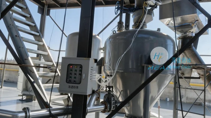
Third, efficiency and scalability are critical considerations. The material handling system must be able to accommodate varying production volumes and different wafer sizes or shapes. This is achieved through modular designs that allow for easy expansion or reconfiguration. The system also integrates with other manufacturing equipment, such as automated loading/unloading stations and robotic arms, to create a seamless workflow. This integration ensures that the material handling process does not become a bottleneck in the overall production line, thereby optimizing throughput and reducing downtime.